- 您现在的位置:买卖IC网 > Sheet目录1993 > DS1347T+ (Maxim Integrated Products)IC RTC/CALENDAR SPI 8TDFN
Low-Current, SPI-Compatible
Real-Time Clock
2
Maxim Integrated
DS1347
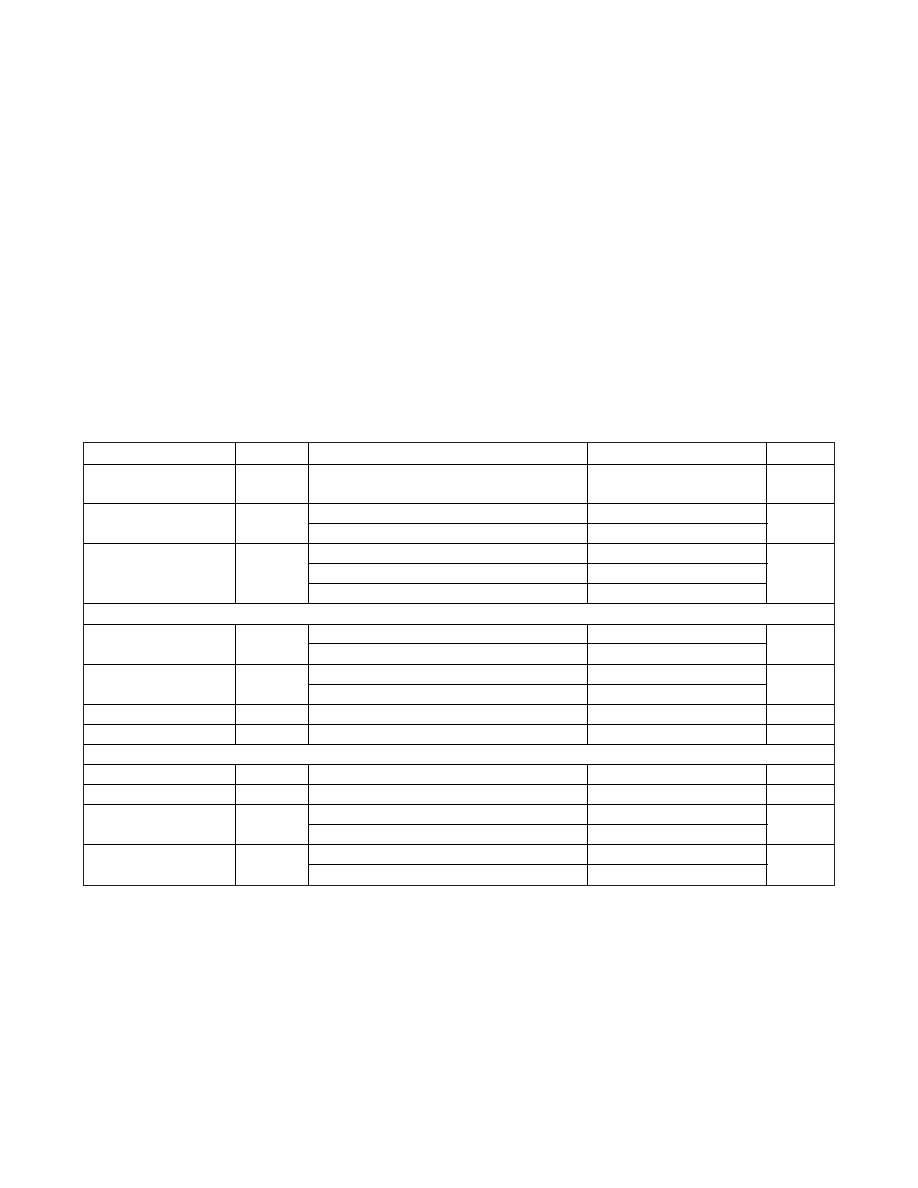
ABSOLUTE MAXIMUM RATINGS
DC ELECTRICAL CHARACTERISTICS
(VCC = +2.0V to +5.5V, TA = -40
°C to +85°C. Typical values are at VCC = +3.3V, TA = +25°C, unless otherwise noted.) (Note 1)
Stresses beyond those listed under “Absolute Maximum Ratings” may cause permanent damage to the device. These are stress ratings only, and functional
operation of the device at these or any other conditions beyond those indicated in the operational sections of the specifications is not implied. Exposure to
absolute maximum rating conditions for extended periods may affect device reliability.
VCC to GND ..............................................................-0.3V to +6V
All Other Pins to GND ................................-0.3V to (VCC + 0.3V)
Current into Any Pin..........................................................±20mA
Rate of Rise, VCC ............................................................100V/s
Continuous Power Dissipation (TA = +70
°C)
TDFN (derate 24.4mW/
°C above +70°C)...................1.375mW
Junction Temperature .....................................................+150
°C
Storage Temperature Range…………………… -55
°C to +125°C
ESD Protection (All Pins, Human Body Model)................±2000V
Lead Temperature (soldering, 10s) .................................+300
°C
Soldering Temperature (reflow) .......................................+260
°C
PARAMETER
SYMBOL
CONDITIONS
MIN
TYP
MAX
UNITS
Operating Voltage
Range
VCC
2
5.5
V
VCC = +2V
0.1
Active Supply Current
(Note 2)
ICC
VCC = +5V
0.25
mA
VCC = +2V
0.35
0.7
VCC = +3.6V
0.35
0.7
Timekeeping Supply
Current (Note 3)
ITK
VCC = +5V
0.4
0.8
μA
SPI DIGITAL INPUTS (SCLK, DIN,
CS)
VCC = +2V
1.4
Input High Voltage
VIH
VCC = +5V
2.2
V
VCC = +2V
0.6
Input Low Voltage
VIL
VCC = +5V
0.8
V
Input Leakage Current
IIL
VIN = 0 to VCC
-0.1
+0.1
μA
Input Capacitance
CIN
(Note 4)
10
pF
SPI DIGITAL OUTPUT (DOUT)
Output Leakage Current
IO
CS = VIH
-0.1
+0.1
μA
Output Capacitance
COUT
(Note 4)
15
pF
VCC = +2V, ISINK = 1.5mA
0.4
Output Low Voltage
VOL
VCC = +5V, ISINK = 4mA
0.4
V
VCC = +2V, ISOURCE = -0.4mA
1.8
Output High Voltage
VOH
VCC = +5V, ISOURCE = -1mA
4.5
V
发布紧急采购,3分钟左右您将得到回复。
相关PDF资料
DS1371U+C01
IC BINARY COUNTER 32-BIT 8-USOP
DS1372U+T&R
IC BINARY COUNTER 32-BIT 8-USOP
DS1374C-3#
IC RTC I2C W/CHARGER 16-SOIC
DS1375T+
IC RTC SERIAL W/ALARM 6-TDFN
DS1384FP-12+
IC CTRLR RTC WDOG 120NS 44-MQFP
DS1386P-8-120+
IC TIMEKEEPER RAM 64K 34-PCM
DS1388Z-3+T&R
IC RTC I2C W/CHARGER 8-SOIC
DS1391U-3+
IC RTC W/CHARGER 10-USOP
相关代理商/技术参数
DS1347T+T&R
制造商:Maxim Integrated Products 功能描述:LOW POWER SPI RTC FOR 12.5PF CRYSTA - Tape and Reel 制造商:Maxim Integrated Products 功能描述:IC RTC/CALENDAR SPI 8TDFN 制造商:Maxim Integrated Products 功能描述:Real Time Clock Low Power SPI RTC For 12.5Pf Crystal
DS1347T+T&R
功能描述:实时时钟 Low Power SPI RTC For 12.5Pf Crystal RoHS:否 制造商:Microchip Technology 功能:Clock, Calendar. Alarm RTC 总线接口:I2C 日期格式:DW:DM:M:Y 时间格式:HH:MM:SS RTC 存储容量:64 B 电源电压-最大:5.5 V 电源电压-最小:1.8 V 最大工作温度:+ 85 C 最小工作温度: 安装风格:Through Hole 封装 / 箱体:PDIP-8 封装:Tube
DS135
制造商:SANYO 制造商全称:Sanyo Semicon Device 功能描述:1.0A Power Rectifier
DS1350AB
制造商:DALLAS 制造商全称:Dallas Semiconductor 功能描述:4096k Nonvolatile SRAM with Battery Monitor
DS1350AB-100
制造商:DALLAS 制造商全称:Dallas Semiconductor 功能描述:4096k Nonvolatile SRAM with Battery Monitor
DS1350AB-70
制造商:DALLAS 制造商全称:Dallas Semiconductor 功能描述:4096k Nonvolatile SRAM with Battery Monitor
DS1350ABL-100
制造商:未知厂家 制造商全称:未知厂家 功能描述:NVRAM (Battery Based)
DS1350ABL-100-IND
制造商:未知厂家 制造商全称:未知厂家 功能描述:NVRAM (Battery Based)